
Mechanical Seal/Silicon Wafer Lapping in South Bend
Precision mechanical seal silicon wafer lapping for South Bend-area programs.
Request a quote. Receive tolerances.
One business day turnaround on South Bend mechanical seal/silicon wafer lapping requests.
Precision mechanical seal silicon wafer lapping for South Bend-area programs.
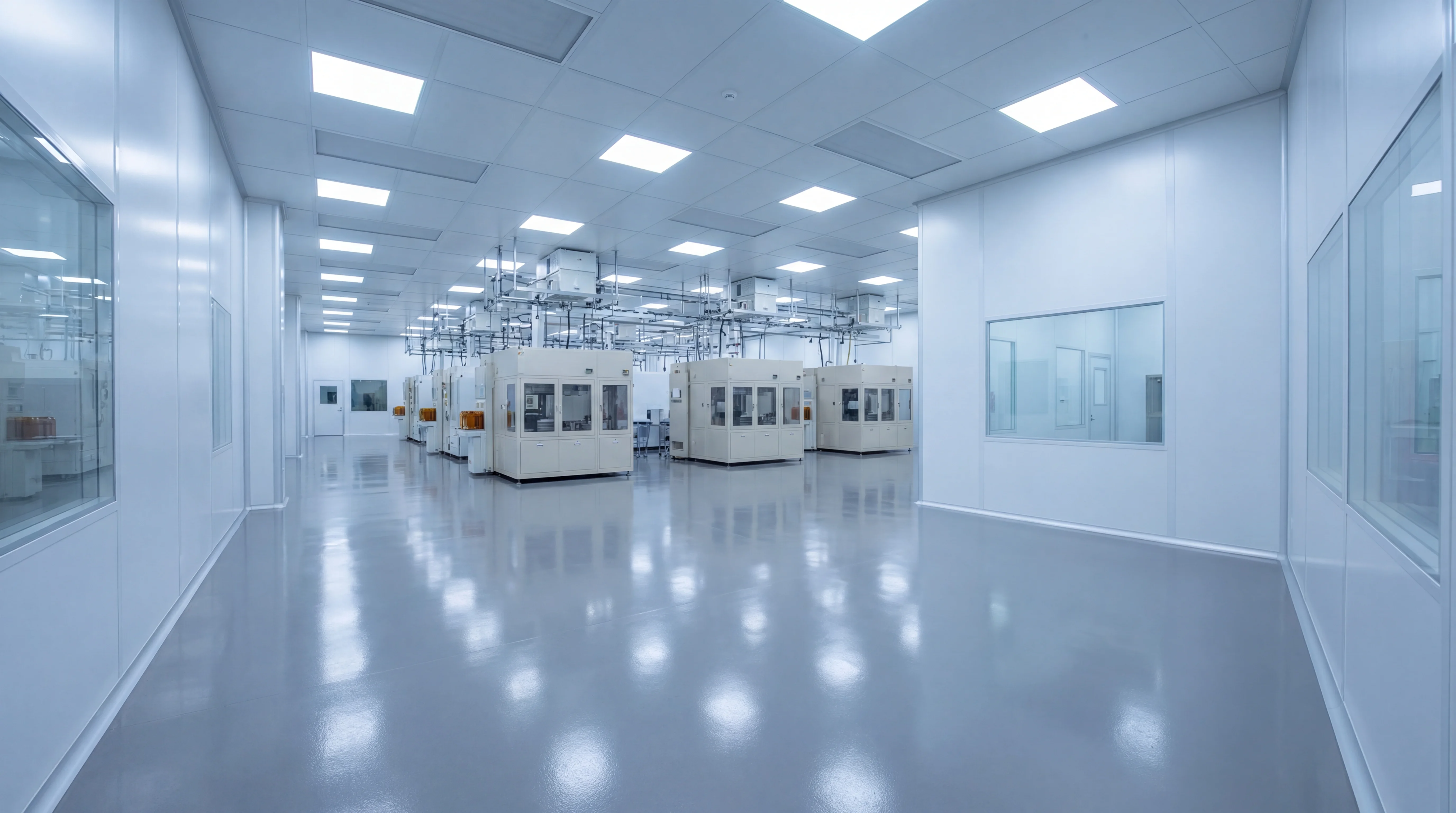
Process Overview
Mechanical Seal/Silicon Wafer Lapping for South Bend-area programs is performed under documented process cards. Each lot is recorded with abrasive type and grit, plate selection, pressure profile, and inspection method so a follow-up lot reproduces the same flatness, parallelism, and Ra. Drawings, target finish, and lot size determine the equipment and the sequence; quotes cover all three together.
Equipment and Process Detail
The equipment configurations below cover mechanical seal/silicon wafer lapping for South Bend-area programs. Click any entry to expand the full specifications, controlled parameters, and typical tolerances.
Cast Iron Lapping Plate (Cross-Hatch Grooved) View specifications
Precision single-sided and double-sided lapping of mechanical seals and silicon wafers relies heavily on conditioned cast iron lapping plates featuring cross-hatch grooved patterns. Gray cast iron, such as Meehanite, provides a ductile and porous matrix ideal for anchoring or "charging" abrasive particles like silicon carbide or diamond slurry. The machined cross-hatch grooves, typically cut at 45-degree or 90-degree intersections, serve critical tribological and operational functions during the flat lapping process:
- Slurry Distribution: Grooves act as micro-channels, ensuring uniform delivery of fresh abrasive media across the entire interface of the workpiece.
- Swarf and Heat Evacuation: Spent abrasives, carrier fluids, and sheared material bypass are constantly channeled away from the cutting zone, preventing scratch defects.
- Surface Tension Mitigation: Grooving prevents hydraulic lock or hydroplaning of thin silicon wafers and highly polished mechanical seal faces, maintaining constant plate-to-part contact.
- Flatness Control: Plate geometry is regularly monitored to achieve flatness tolerances within one to two helium light bands (0.3 to 0.6 microns) in accordance with ASME B46.1 surface texture standards.
Diamond Lapping Plate (Kemet Plate / Diamond System) View specifications
Diamond lapping plates, including composite structures such as Kemet plates, are utilized to achieve extreme flatness and precise surface finishes on exceptionally hard substrates, including silicon wafers, tungsten carbide, and ceramic mechanical seal faces. Unlike conventional cast iron lapping systems that rely on rolling, loose abrasives suspended in a high-volume slurry, diamond plate systems employ a specialized matrix that securely holds micron-graded diamond particles. This fixed-abrasive methodology embeds the cutting media directly into the lap surface, which optimizes the material removal rate while significantly minimizing subsurface damage and preventing abrasive impregnation within the processed workpiece.
Flatness tolerances measured in fractions of a helium light band and surface roughness (Ra) values descending into the nanometer range are routinely maintained using these systems. The implementation of a diamond plate architecture is critical for both single-sided and double-sided lapping operations where stringent parallelism, exacting thickness controls, and optical-grade reflectivity are mandated by specifications. Operational parameters for diamond plate lapping generally include:
- Consistent abrasive exposure to ensure uniform material removal across the entire workpiece batch.
- Precise conditioning routines utilizing facing rings to maintain absolute plate flatness and kinematic stability.
- Controlled application of specialized water-based or oil-based lubricants to manage thermal expansion and facilitate swarf removal.
- The capability to process composite or dissimilar materials simultaneously without preferential edge wear or edge roll-off.
Double-Side Wafer Lapping Machine View specifications
Double-side lapping machines utilize a planetary kinematic motion to process both faces of a silicon wafer or mechanical seal simultaneously. Workpieces are nested within geared carriers that rotate between upper and lower counter-rotating lap plates. An abrasive slurry, typically composed of suspended silicon carbide or aluminum oxide, is continuously delivered to the processing zone. By abrading both surfaces concurrently, built-in stress and subsurface damage from initial slicing operations are effectively removed. This simultaneous stock removal is critical for achieving exceptional global flatness and minimizing Total Thickness Variation (TTV) across the entire substrate diameter.
Strict control over plate condition and slurry distribution is maintained to meet tight geometric tolerances and conform to relevant SEMI standards for semiconductor materials. Typical parameters optimized during double-side lapping operations include:
- Total Thickness Variation (TTV): Maintained within micron or sub-micron tolerances to ensure downstream photolithography precision.
- Parallelism and Flatness: Regulated to provide uniform geometry prior to chemical mechanical planarization (CMP).
- Surface Roughness (Ra): Controlled material removal rates yield a consistent, uniform matte finish suitable for subsequent polishing phases.
- Bow and Warp: Minimized through equalized kinetic friction and balanced, dual-sided pressure distribution across the wafer surface.
Single-Side Wafer Lapping Machine View specifications
Single-side wafer lapping equipment is utilized to achieve stringent flatness and surface finish requirements on one face of a substrate, typically for silicon wafers and mechanical seal faces. Material removal is accomplished by placing components inside conditioning rings on a rotating lapping plate while an abrasive slurry is continuously introduced. Downward pressure is applied via rigid pressure plates, ensuring uniform contact between the workpiece and the lapping surface. This process reduces surface irregularities, removes subsurface damage from primary slicing, and establishes a precise geometric datum plane before subsequent precision polishing operations are executed.
When single-side lapping is performed, critical parameters are tightly controlled to align with industry specifications such as SEMI standards for semiconductor materials or ASME B46.1 for surface texture. Operational controls and capabilities typically include:
- Flatness (TIR): Geometry is controlled to within helium light bands, frequently achieving tolerances of less than 0.00001 inches (0.25 microns) depending on the substrate diameter.
- Surface Finish (Ra): Predictable roughness averages are generated to prepare component surfaces for final chemical-mechanical planarization (CMP) or high-pressure sealing.
- Material Compatibility: The kinematic abrasive process is effectively applied to hard and brittle materials, including silicon carbide, tungsten carbide, and alumina ceramics.
- Plate Conditioning: Cast iron or composite lapping plates are continuously conditioned during the cycle to maintain a strictly flat profile, mitigating localized wear.
Additional Equipment and Variants
Other configurations available for mechanical seal/silicon wafer lapping — expand any item below for selection notes.
15" Diameter Seal Lapping Machine (Up To ~125 mm Seals)
15" Diameter Seal Lapping Machine (Up To ~125 mm Seals) is selected when part size, materials, or surface finish targets call for that specific platform. Setup is recorded on the per-lot travel sheet so subsequent lots reproduce the same conditions.
24" Diameter Seal Lapping Machine (Up To ~200 mm Seals)
24" Diameter Seal Lapping Machine (Up To ~200 mm Seals) is selected when part size, materials, or surface finish targets call for that specific platform. Setup is recorded on the per-lot travel sheet so subsequent lots reproduce the same conditions.
Ceramic Conditioning Ring
Ceramic Conditioning Ring is selected when part size, materials, or surface finish targets call for that specific platform. Setup is recorded on the per-lot travel sheet so subsequent lots reproduce the same conditions.
Diamond Spray / Slurry Dispensing System
Diamond Spray / Slurry Dispensing System is selected when part size, materials, or surface finish targets call for that specific platform. Setup is recorded on the per-lot travel sheet so subsequent lots reproduce the same conditions.
Vertical Wafer Grinding Machine (Hvg Series)
Vertical Wafer Grinding Machine (Hvg Series) is selected when part size, materials, or surface finish targets call for that specific platform. Setup is recorded on the per-lot travel sheet so subsequent lots reproduce the same conditions.
Pyrex Glass Lapping Plate
Pyrex Glass Lapping Plate is selected when part size, materials, or surface finish targets call for that specific platform. Setup is recorded on the per-lot travel sheet so subsequent lots reproduce the same conditions.
Ceramic Conditioning Ring (Wafer Carrier)
Ceramic Conditioning Ring (Wafer Carrier) is selected when part size, materials, or surface finish targets call for that specific platform. Setup is recorded on the per-lot travel sheet so subsequent lots reproduce the same conditions.
Backlapping / Thinning Fixture
Backlapping / Thinning Fixture is selected when part size, materials, or surface finish targets call for that specific platform. Setup is recorded on the per-lot travel sheet so subsequent lots reproduce the same conditions.
Materials and Tolerances
Common materials for mechanical seal/silicon wafer lapping include hardened tool steels, stainless alloys, tungsten carbide, ceramics (Al₂O₃, ZrO₂, SiC), single-crystal silicon, sapphire, and carbon-graphite seal faces. Flatness targets of one light band (~11.6 µin / 0.3 µm) are routine; sub-micron parallelism is held on planetary fixtures with matched carriers.
Inspection and Certification
In-process inspection uses interferometer plates for flatness, profilometers for Ra, and gauge blocks or air gauges for dimensional checks. Per-lot certification is issued on production runs and ties measured results back to the originating drawing and travel sheet.