
Chicago Lapping Co
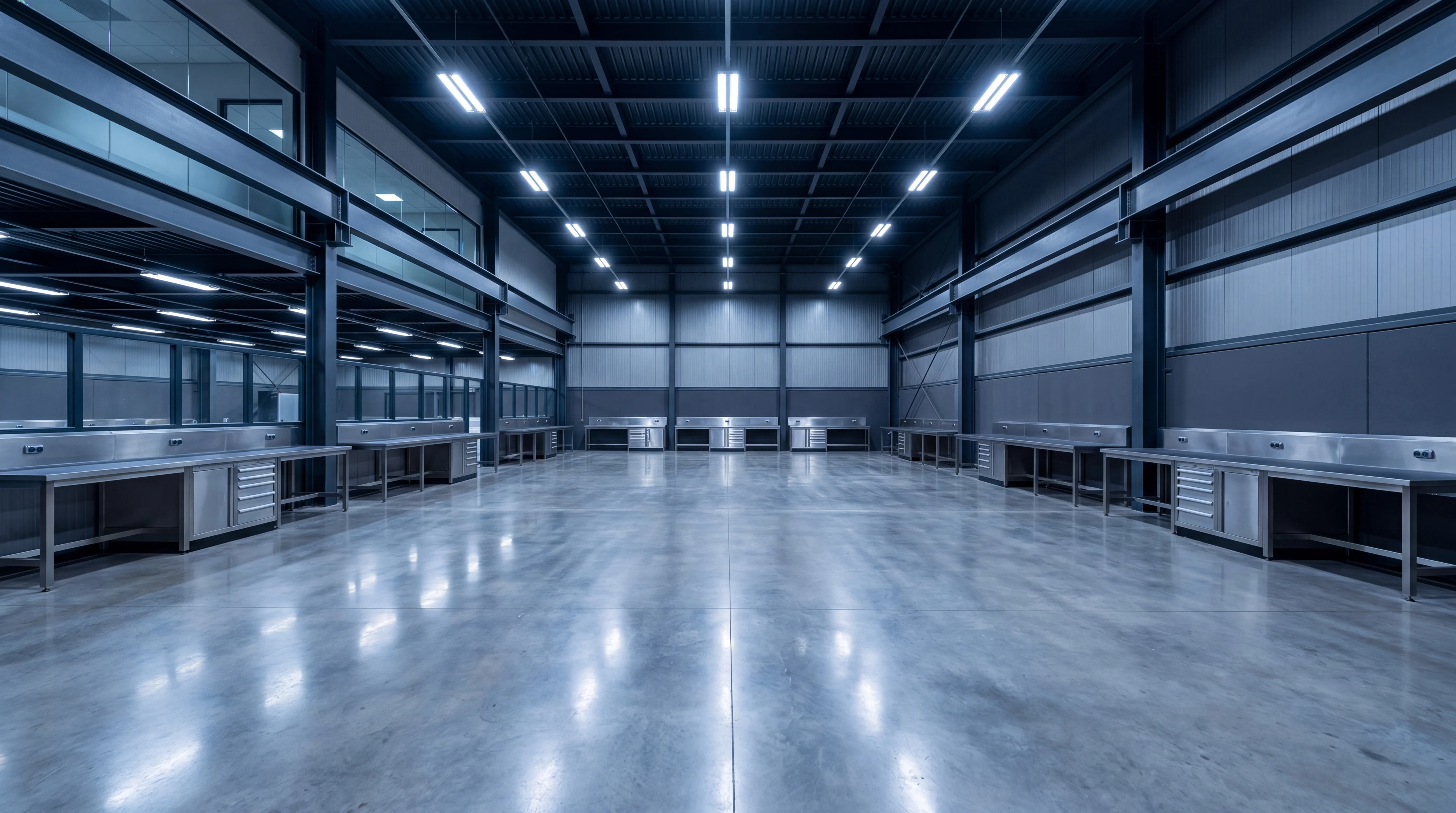
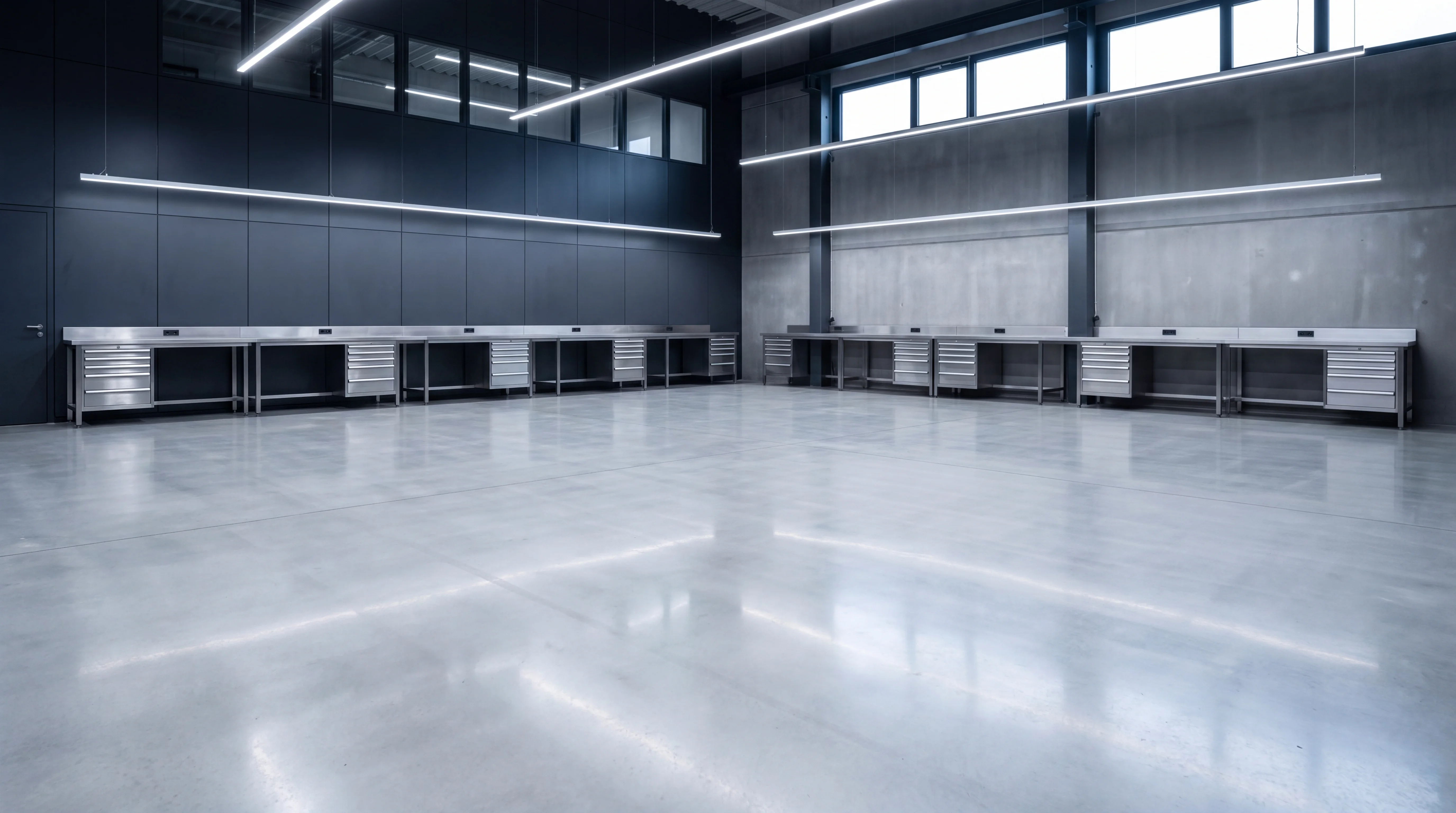
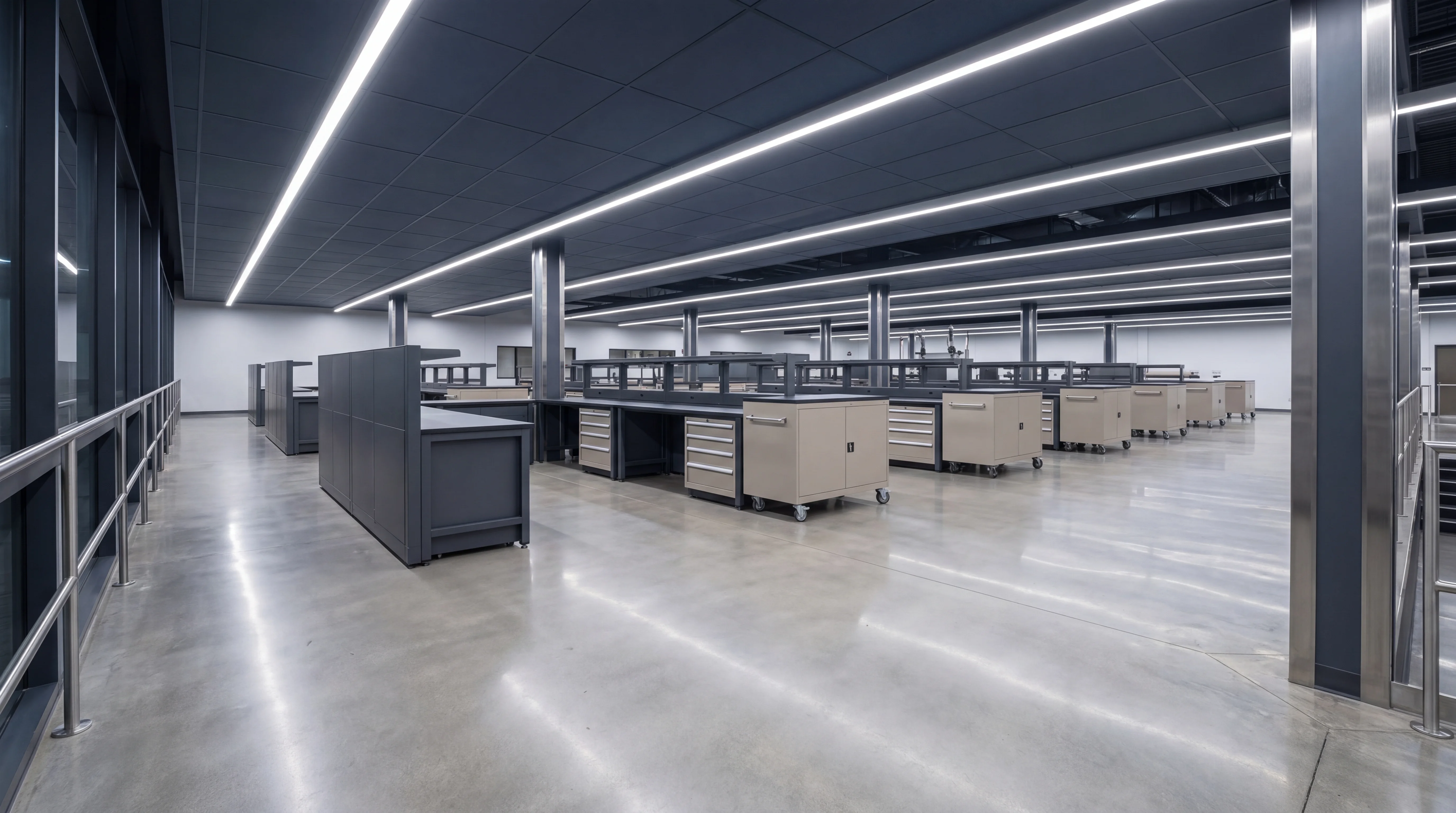
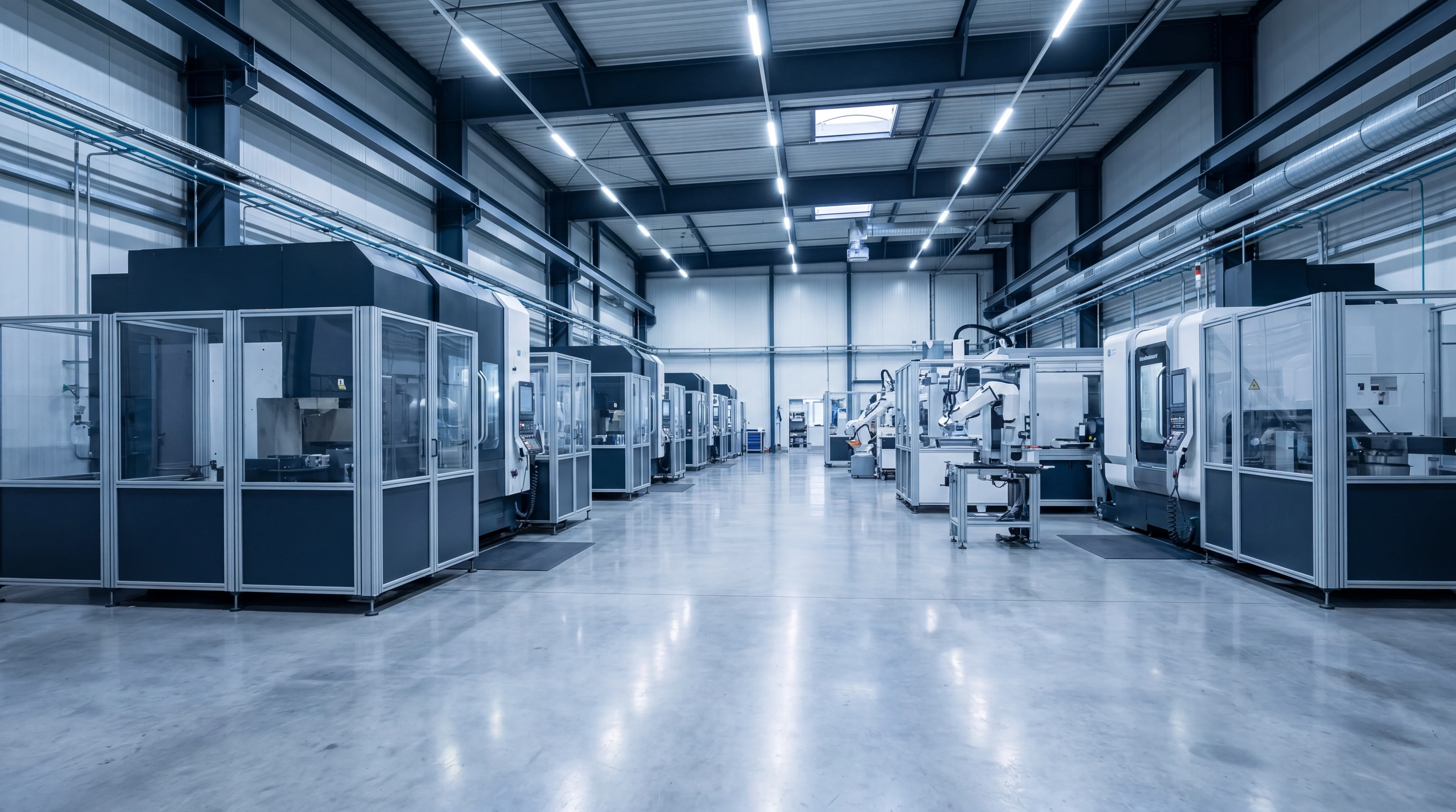
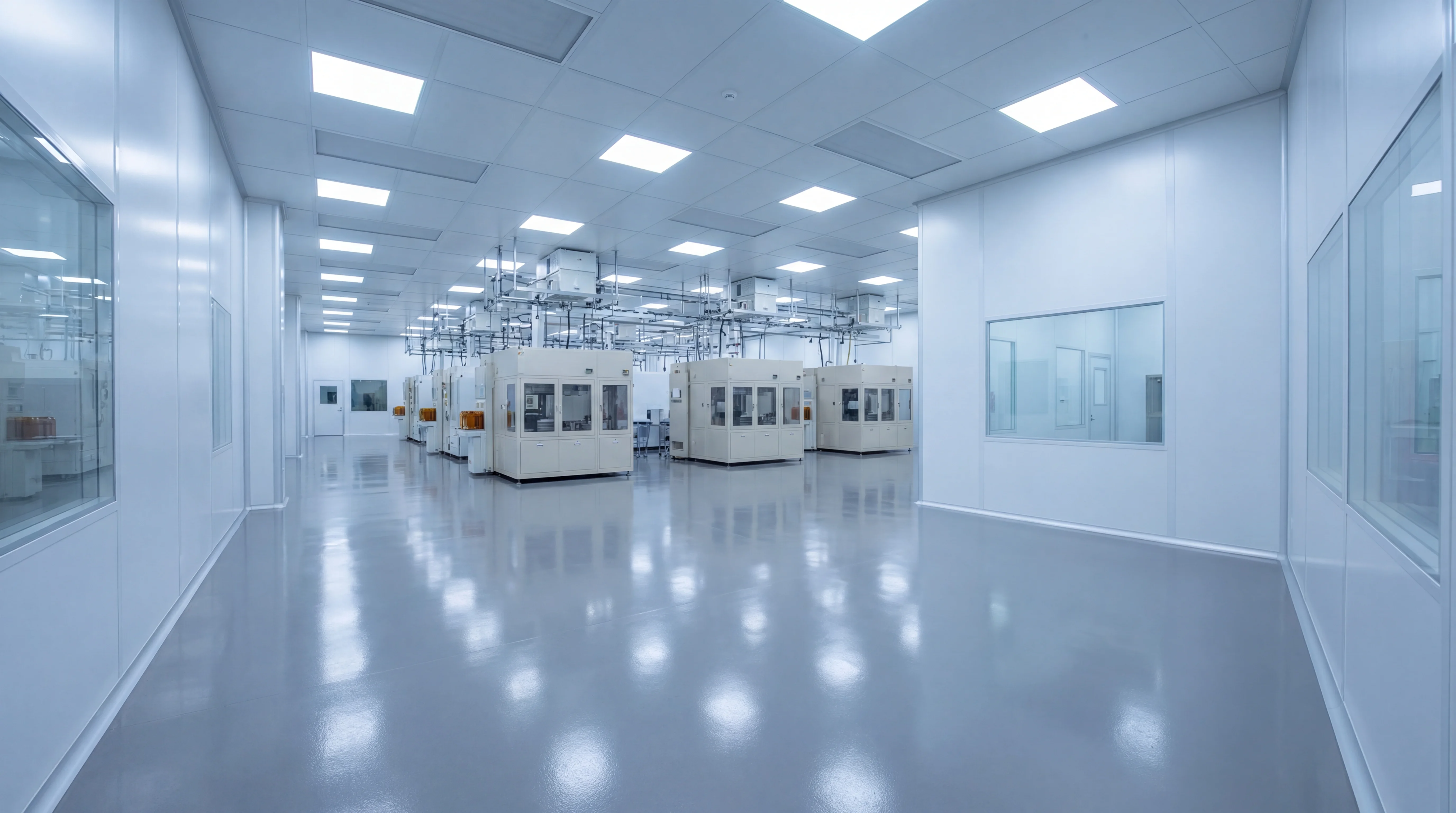
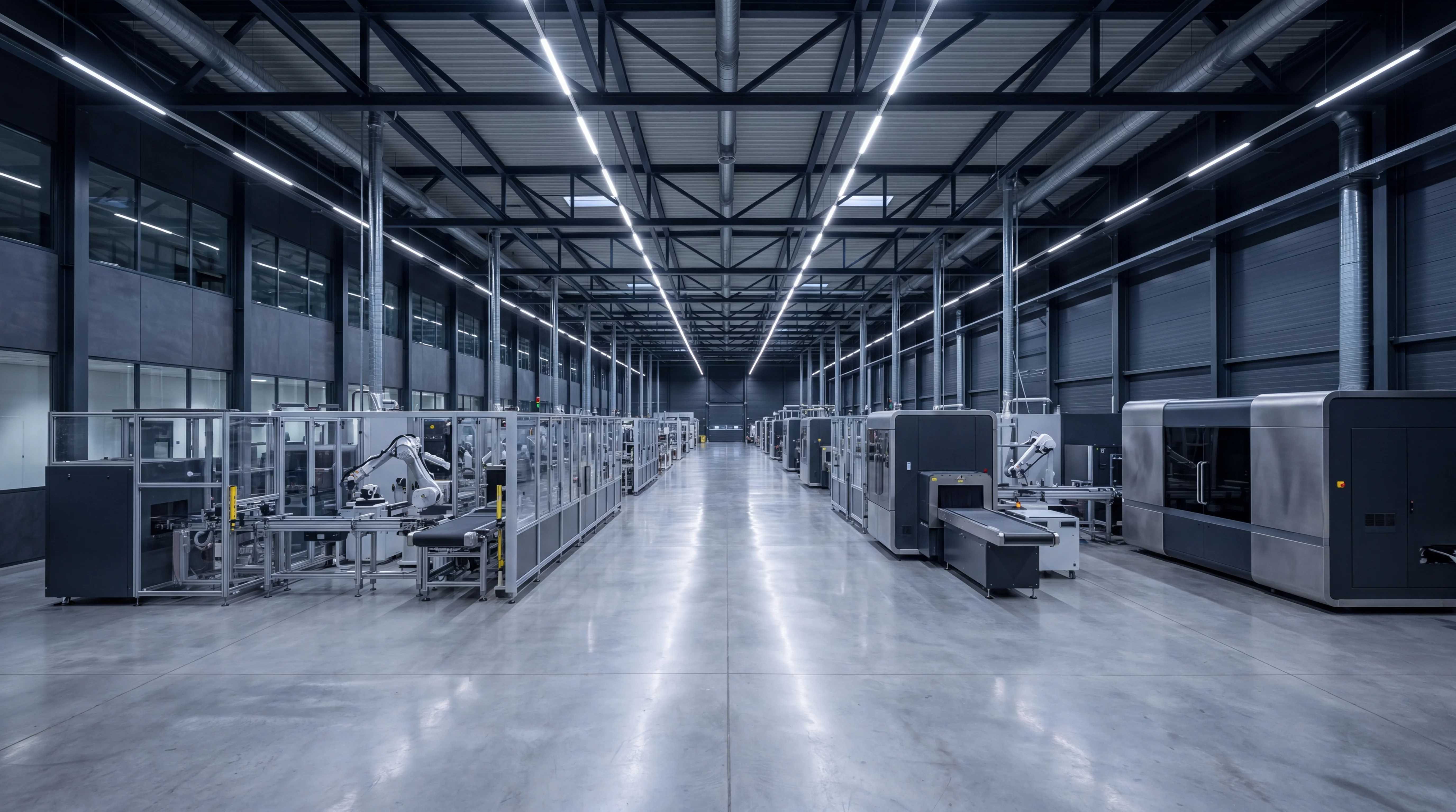
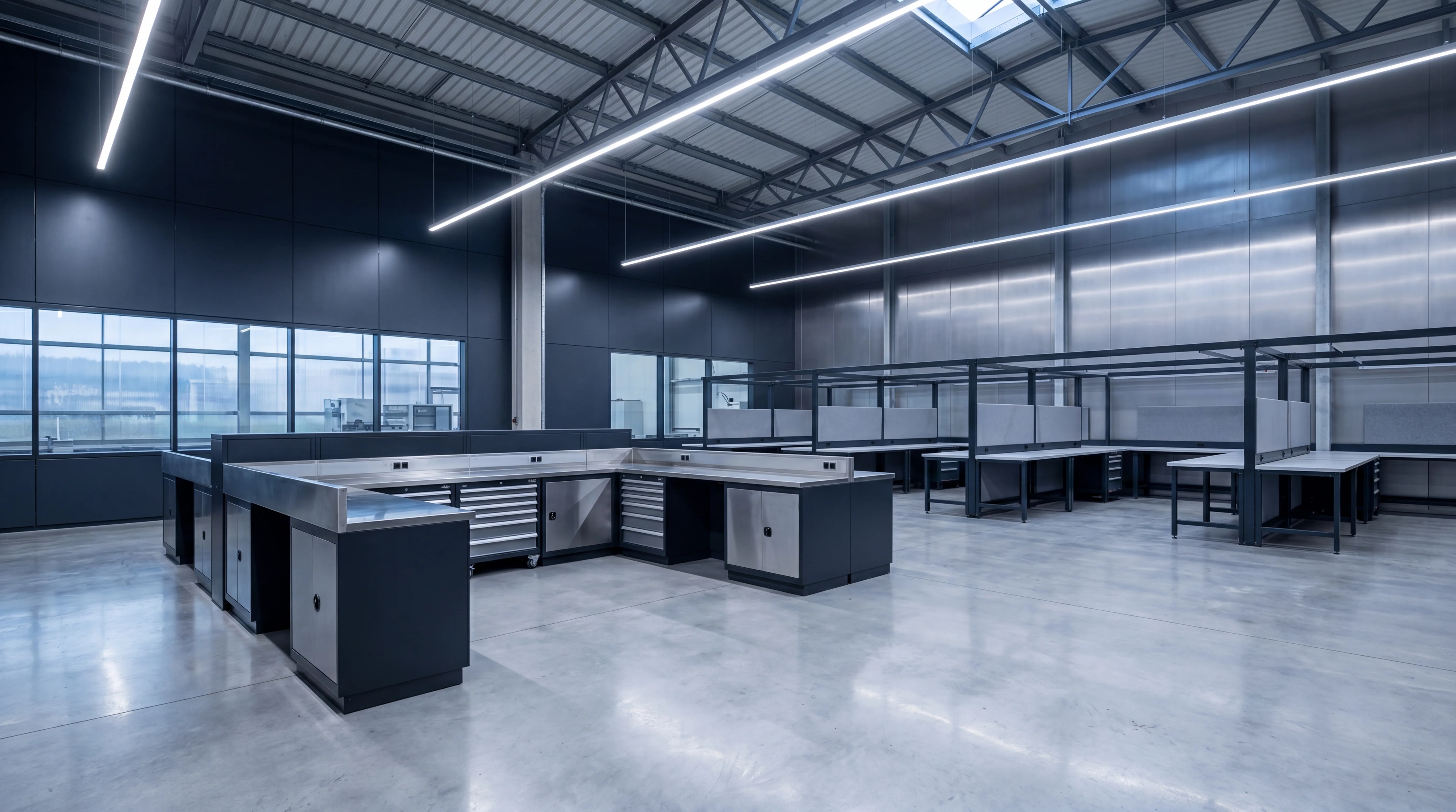
Contract precision lapping for Chicago-area aerospace, semiconductor, and medical programs. Single & double-sided lapping, flat honing, mechanical-seal and wafer finishing — held to light-band flatness on production volumes.
Core Capabilities
Every lapping process below is available across Illinois, Wisconsin & Indiana, performed under documented process controls aligned with ISO 9001:2015. Submit one request and receive a direct quote covering process selection, tolerances, and lead time within one business day.
Single and Double-Sided Lapping
Precision single and double-sided lapping held to light-band flatness and µin-level surface finish.
Flat lapping
Precision flat lapping held to light-band flatness and µin-level surface finish.
Spherical/Ball Lapping
Precision spherical/ball lapping held to light-band flatness and µin-level surface finish.

Hand lapping
Precision hand lapping held to light-band flatness and µin-level surface finish.
Machine lapping
Precision machine lapping held to light-band flatness and µin-level surface finish.
Mechanical Seal/Silicon Wafer Lapping
Precision mechanical seal/silicon wafer lapping held to light-band flatness and µin-level surface finish.
Production lapping
Precision production lapping held to light-band flatness and µin-level surface finish.
Taper, Shoulder, and Counter Bore Lapping
Precision taper, shoulder, and counter bore lapping held to light-band flatness and µin-level surface finish.
Verifiable Precision
Flatness is not asserted — it is measured. Each lot is verified on temperature-stabilized metrology benches combining laser interferometry, white-light profilometry, and air gaging. Every micron is traceable to a calibrated standard.
- Laser InterferometryFlatness / Form
- White-Light Profilometry3D Surface Texture
- Stylus ProfilometerRa / Rz Roughness
- Air GagingThickness / Parallelism
Proof, Not Claims
Coverage breadth, certified processes, and traceable inspection — surfaced as datasheet numbers, not marketing copy.
Tolerances Achievable By Material Class
| Material Class | Typical Applications | Min Thickness | Flatness | Ra |
|---|---|---|---|---|
| Technical Ceramics (Al₂O₃, AlN) | Semiconductor chucks, seals | 0.005" | 1 light band | < 1 µin |
| Silicon Carbide (SiC) | Optics, wafer handling | 0.010" | 1/4 light band | < 0.5 µin |
| Tool Steels / Tungsten Carbide | Stamping dies, cutting tools | 0.002" | 2 light bands | < 2 µin |
| Exotic Alloys (Ti, Inconel) | Aerospace components, medical | 0.015" | 2 light bands | < 4 µin |
| Optical Materials (Sapphire, Fused Silica) | Windows, lenses, substrates | 0.004" | 1/10 light band | Sub-angstrom |
| Silicon Wafers | CMP, bonding, MEMS substrates | 0.005" | 1/4 light band | < 0.5 µin |
Chicago Lapping Co Service Areas
Precision lapping coverage spans Illinois , Wisconsin , and Indiana , with dedicated landing pages for every metropolitan area in the index below.
View metropolitan coverage list
Local-pickup and freight coverage includes Chicago , Aurora , Schaumburg , Elgin , Joliet , Rockford , Milwaukee , Madison , Green Bay , Kenosha , Racine , Appleton , Waukesha , Indianapolis , Fort Wayne , Evansville , South Bend , and Hammond . Each city page covers the lapping processes available in that metro, typical lead times, and how to submit for a direct quote.
REGION: Illinois, Wisconsin & Indiana · 3 STATES · 18 METROS
Coverage Network Where Work Is Performed
Request A Quote, Receive Tolerances
Quotes typically returned within one business day. Include drawings, target finish, and lot size — the response covers achievable flatness, lead time, and pricing for the part geometry.
- Direct line(618) 323-0428
- Emailjack@chicagolappingservices.com
- HoursMon – Fri / 07:00 – 17:00 CT
- Turnaround≤ 1 business day